深圳市亿泰信电子有限公司
(The purpose of this YTX300H/YTX300 SPECcovers mainly for the hardware and RFparameterinfo of the module,For software infoplease refer toYX300 chip datasheets anddemo program of YTXDuino (rm) Develo -pmentKit)
1. General introduction
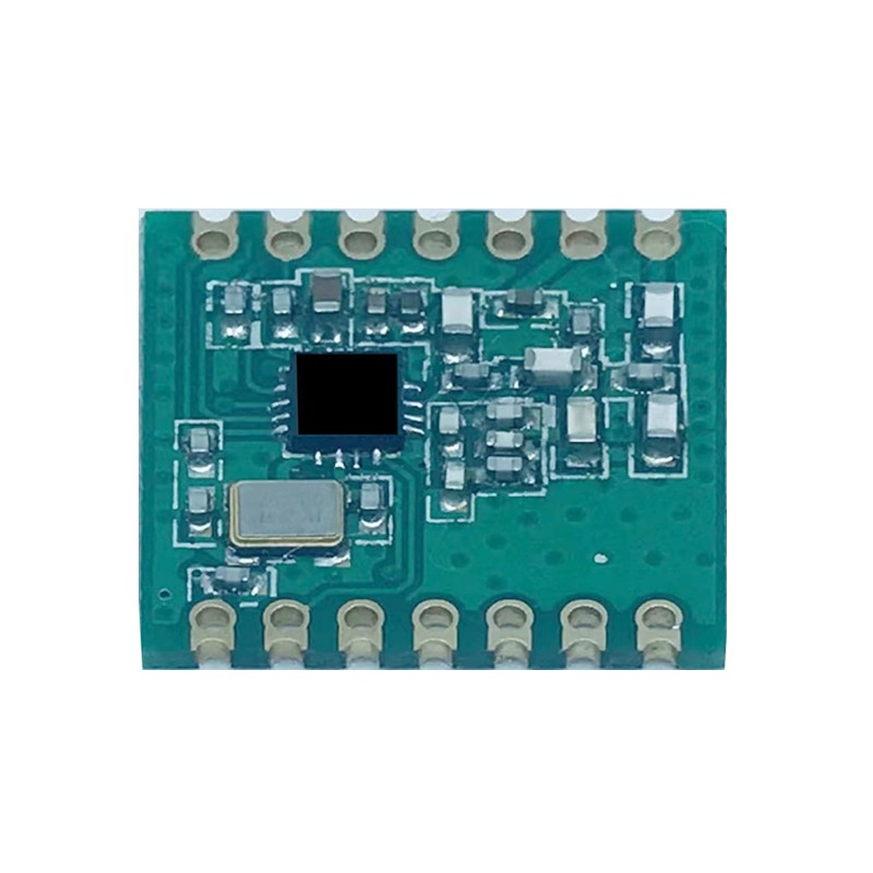
YTX 300H/YTX300module series’ design is based on thehigh performanceCMOSTEK NextGenRF TM YTX300chip, ltoperate at 433/868/915MHz ISM band , The lowreceive sensitivity(-120dBm)coupled with +20dBm(YTX300H)/+13dBm(YTX300)output power ensuresextended range and improved link performance.
2. Features:
140dB maximum link budget.
Low RX current of 7mA.
+20 dBm output power @YTX300H;+13 dBm output power @YTX300Programmable bit rate up to 300 kbps@FSK/40 kbps@OOK
High sensitivity: down to -120dBm.
FSK, GFSK, and OOK modulation.
SMD Package (16x16X1.8
3.Application:
Meter Reading
Wireless data collection
Home automation and
Pin Definition:
YTX300H Pin Definition
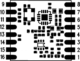
FFiigure 1. YTX300H Pin Definition
|
Number |
Definition |
Type |
Function |
|
1 |
ANT |
AI/ AO |
RF signal input/output. |
|
2 |
GND |
G |
Ground. |
|
3 |
TX-ANT |
I/O |
Tx Antenna sseelect iinnppuutt ppiinn, When YTX300H is TX state,TX_ANT should be = 0, RX_ANT should be =1 |
|
4 |
RX-ANT |
I/O |
Rx Antenna select input pin, When YTX300 IS RX state,RX_ANT should be = 0, TX_ANT should be = 1 |
|
5 |
3.3V(VDD) |
PI |
Power supply input,1.8-3.6V. |
|
6 |
GPIO1 |
I/O |
General Purpose Digital I/O that may be configured through the registers to perform variousfunctions |
|
7 |
GPIO2 |
||
|
8 |
GPIO3 |
||
|
9 |
GND |
G |
Ground. |
|
10 |
SDIO |
I/O |
SPI Data input and output. |
|
11 |
CSB |
I |
SPI Chip select input, active low. |
|
12 |
SCK |
I |
SPI Clock input. |
|
13 |
FCSB |
I |
SPI FIFO select input, active low. |
|
14 |
NC |
|
No Connect. |
|
15 |
NC |
|
No Connect. |
|
16 |
GND |
G |
Ground. |
YTX300 Pin Definition
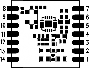
Figure 2. YTX300 Pin Definition
|
Number |
Definition |
Type |
Function |
|
1 |
ANT |
AI/ AO |
RF signal input/output. |
|
2 |
3.3V(VDD) |
PI |
Power supply input,1.8-3.6V. |
|
3 |
GND |
G |
Ground. |
|
4 |
NC |
|
No Connect. |
|
5 |
CSB |
I |
SPI Chip select input, active low. |
|
6 |
SCK |
I |
SPI Clock input. |
|
7 |
FCSB |
I |
SPI FIFO select input, active low. |
|
8 |
SDIO |
I/O |
SPI Data input and output. |
|
9 |
GPIO1 |
I/O |
General Purpose Digital I/O that may be configured through the registers to perform variousfunctions |
|
10 |
GPIO3 |
||
|
11 |
GPIO2 |
||
|
12 |
NC |
|
No Connect. |
|
13 |
NC |
|
No Connect. |
|
14 |
GND |
G |
Ground. |
Electrical :
Maximum
|
parameter |
minimum |
|
Unit |
|
Positive Power Supply |
-0.3 |
|
V |
|
Voltage O |
-0.3 |
+ 0.3 |
V |
|
Voltage On Analog Inputs |
-0.3 |
+ 0.3 |
V |
|
RX Input Power |
- |
|
d℃Bm |
|
Storage Temperature |
-55 |
+ 25 |
℃ |
|
Soldering Temperature(10s) |
- |
+ 55 |
|
|
|
-2 |
|
KV |
|
parameter |
minimum |
|
Unit |
|
Positive Power Supply |
+1.8 |
|
V℃ |
|
Working Temperature |
-40 |
|
|
|
Supply Voltage Slew Rate |
1 |
- |
mV/us |
DC characteristic
|
parameter |
conditions |
minimum |
|
maximum |
Unit |
|
YTX300H |
433MHz band, Pout =+20dBm |
- |
75 |
100 |
mA |
|
TX WorkingCurrent |
868MHz band, Pout =+20dBm |
- |
80 |
100 |
|
|
|
915MHz band, Pout =+20dBm |
- |
85 |
100 |
|
|
YTX300 |
433MHz band, Pout =+13dBm |
- |
28 |
45 |
mA |
|
TX WorkingCurrent |
868MHz band, Pout =+13dBm |
- |
30 |
45 |
|
|
|
915MHz band, Pout =+13dBm |
- |
30 |
45 |
|
|
YTX300H/YTX300 |
433MHz band, |
- |
7 |
10 |
mA |
|
RX WorkingCurrent |
868MHz band, |
- |
7.5 |
10.5 |
|
|
|
915MHz band, |
- |
7.5 |
10.5 |
|
|
YTX300H/YTX300 Sleep Current |
All band |
- |
- |
1 |
uA |
|
parameter |
conditions |
minimum |
typical |
maximum |
Unit |
|
TX Frequency Range Programmable |
433 MHz band, 868 MHz band, 915 MHz band, |
413 848 895 |
- - - |
453 888 935 |
MHz |
|
YTX300H Output Power |
433/868/915MHz band |
- |
+20 |
- |
dBm |
|
YTX300 Output Power |
433/868/915MHz band |
- |
+13 |
- |
dBm |
|
Symbol Rate, FSK Mode |
Programmable |
0.1 |
- |
300 |
kbps |
|
SymbolRate, OOK Mode |
Programmable |
0.1 |
- |
40 |
kbps |
|
Frequency Deviation,FSK |
Programmable |
1 |
- |
200 |
KHz |
|
Frequency Resolution |
|
- |
24.8 |
- |
Hz |
|
parameter |
conditions |
minimum |
typical |
maximum |
Unit |
|
RX Frequence Range |
433 MHz band, |
413 |
- |
453 |
MHz |
|
Programmable |
868 MHz band, |
848 |
- |
888 |
|
|
|
915 MHz band, |
895 |
- |
935 |
|
|
RX Sensitivity |
433MHz |
- |
-120 |
- |
dBm |
|
OOK ModeSR =1.2 kbps, |
868MHz |
- |
-118 |
- |
|
|
|
915MHz |
- |
-118 |
- |
|
|
RX Sensitivity |
433MHz |
- |
-118 |
- |
dBm |
|
FSK ModeFDEV = 19.2 kHz, S |
868MHz |
- |
-116 |
- |
|
|
=1.2 kbps, |
915MHz |
- |
-116 |
- |
|
|
Receiver Bandwidth |
|
50 |
|
500 |
KHz |
|
Blocking Immunity |
+/-1MHz offset |
- |
52 |
- |
dB |
|
|
+/-2MHz offset |
- |
74 |
- |
|
|
|
+/-10MHz offset |
- |
75 |
- |
|
|
Image Rejection Ratio |
IF=280KHz |
- |
35 |
- |
dB |
Typical A :
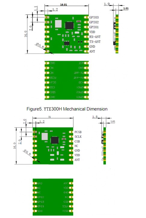
Figure 3. YTX300HApplication
Figure 4. YTX300 Application
(Foorr software info please refer toYTX300 chip datasheets and demo program of
YTXDuinoTM Development Kit)
7.(All units in mm)
8.
|
Model |
Frequencyband |
O |
|
YTX300H-433S2 |
433MHZ |
|
|
YTX300H-868S2 |
868MHZ |
|
|
YTX300H-915S2 |
915MHZ |
|
|
YTX300-433S2 |
433MHZ |
|
|
YTX300-868S2 |
868MHZ |
|
|
YTX300-915S2 |
915MHZ |
|